Q*bert Video Repair
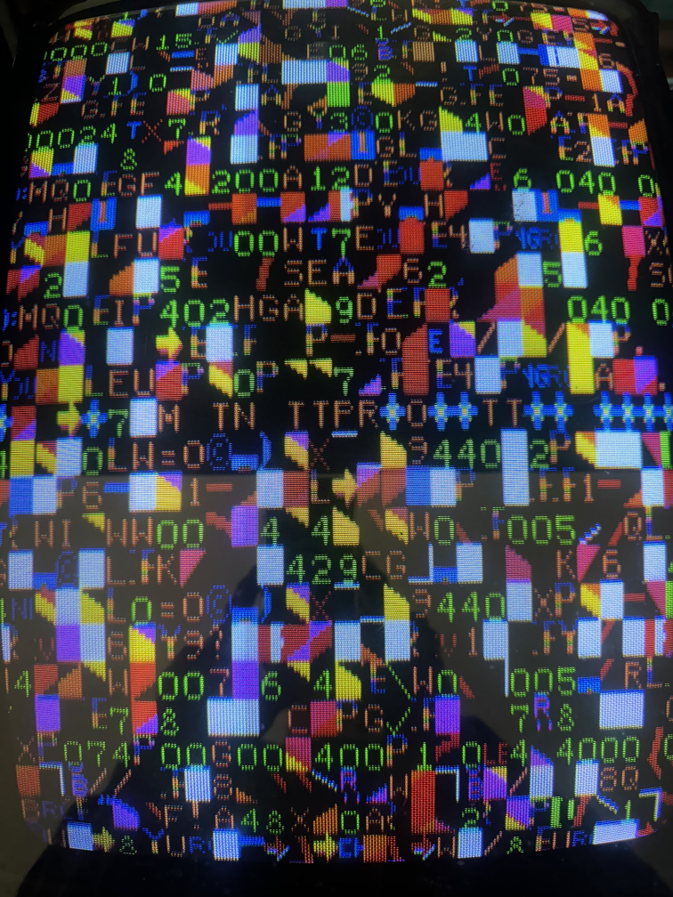
After booting up the board in attract mode, it looked like this. The game was playing, but the video was scrambled.
While looking at the schematics to determine a starting point, I saw that JP21 can be used to override foreground and background selection. If the jumper is moved to JP22, only the foreground video will be visible. If the jumper is removed and JP21 is pulled high, only the background will be display.
| Background | Foreground |
|
|
The background tiles were rendering properly, but garbage was being selected to draw. The foreground sprites were being chosen correctly, but t hey were missing random lines when being drawn. It appeared there were different problems in both areas of the hardware.
I decided to start with the background issue, comparing the background video RAM against MAME. A 74HC138 at B6 is used to control access to the video RAM based on the values in address bits 11, 12, and 13.
| signal | pin | binary address | hex address | RAM chip(s) |
| FRSEL | Y6 | 11 0000 0000 0000 | 0x3000 | E4, E1-2, E2-3 |
| BRSEL | Y7 | 11 1000 0000 0000 | 0x3800 | E7 |
BRSEL is used to select the background video RAM, which is chip E7. In the schematics, this chip is labeled "Background Character Register" and is addressed at 0x3800 - 0x3fff. In MAME, this address range is referred to as "video RAM."
Background Video
I entered the service menu in MAME and set a watchpoint on writes to the video RAM address that corresponds to E7 at 0x3800. After the menu is loaded, only one byte is written to the background RAM every few frames to make the cursor blink. The write address was 0x3872, and the value being written alternated between 0xBD and 0xBE.
> wpset 3800,7ff,w
Watchpoint 1 set
Stopped at VBLANK
Stopped at watchpoint 1 writing BE to 03872 (PC=0DBBD)
Stopped at VBLANK (20x)
Stopped at watchpoint 1 writing BD to 03872 (PC=0DBBD)
Stopped at VBLANK (20x)
Stopped at watchpoint 1 writing BE to 03872 (PC=0DBBD)
Stopped at VBLANK
I went back to the physical hardware, connected my logic analyzer to E7 and ran a capture. After decoding the recorded signals, the data values were correct, but the write address was 0x70, which should have been 0x72 according to the behavior in MAME.
WR 70, bd
WR 70, be
The lower 4 bits of the address sent to E7 is latched from the data bus through a 74ls157 chip at D7.
I hooked up the logic analyzer to D7, and it showed that the inputs into the latch matched expectations, but the outputs were not correct.
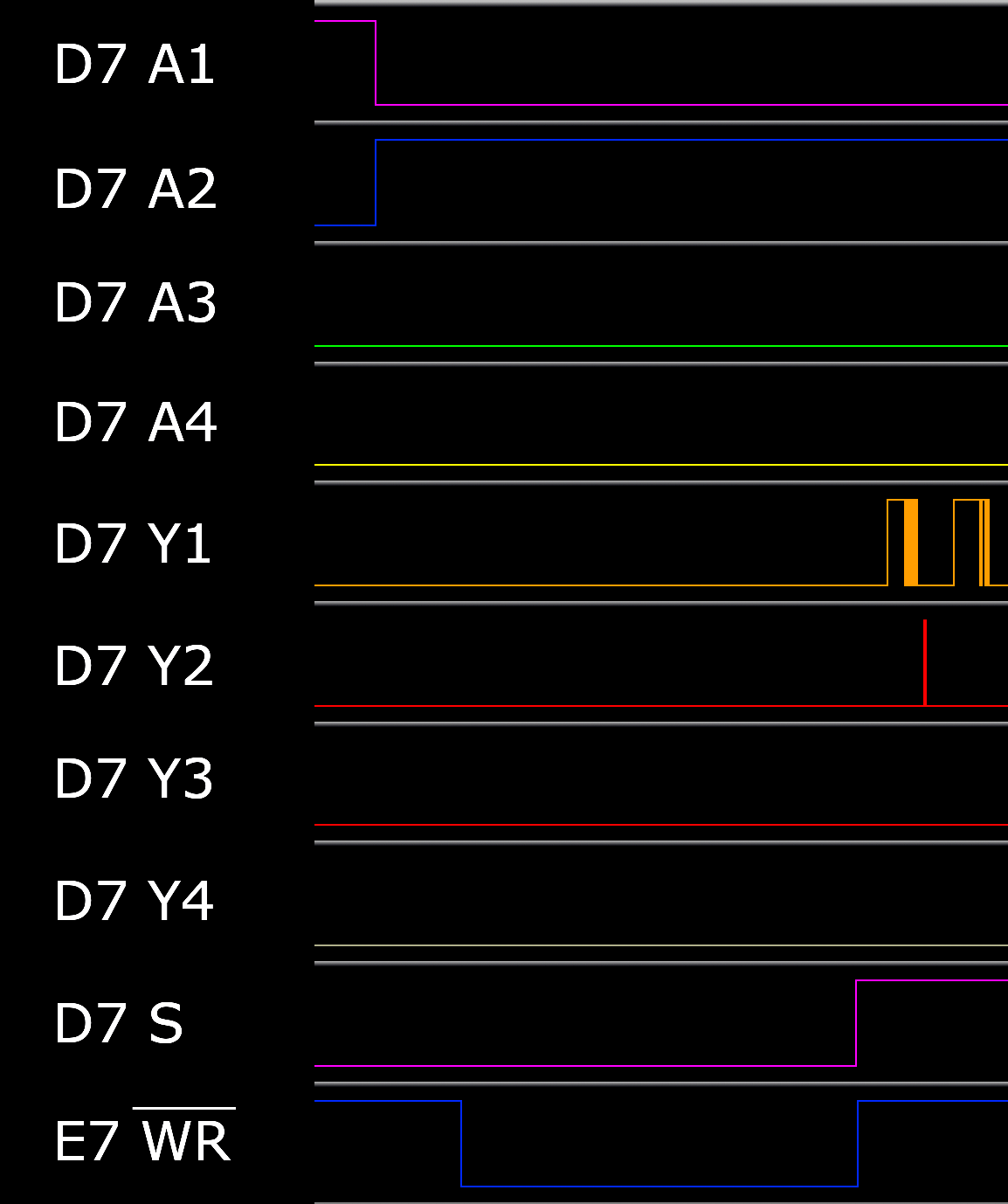
When S is low, the Y outputs should match the A inputs. The captured data showed that during the write operation to E7, S was low, A2 was high, but Y2 remained low.
I Replaced D7 and the background video was fixed.
That was unexpectedly Easy!
Foreground Video
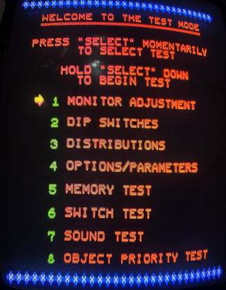
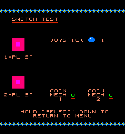
The foreground objects were more complicated.To begin analyzing the behavior of the sprites, I wanted a static screen in the game where I could deterministically reproduce the data behavior over multiple captures. The service menu doesn't draw any sprites, but fortunately, digging into the menu, the switch test renders exactly one static sprite representing the position of the joystick.
per the gfx_layout in MAME, sprites are stored as follows
| width | 16 |
| height | 16 |
| planes | 4 |
| stride | 32 bytes |
Combining the graphics layout from MAME with the schematics, I was able to derive the following logic for decoding sprites.
- Each pixel is stored 1 bit per ROM across 4 ROMs.
- Each ROM holds 8 bits of data at 13 bit addresses.
- Each sprite is encoded 2 bytes per line per ROM over 16 lines.
- At each sample, 8 bits are read from each ROM that are loaded into a dedicated 74ls166 per ROM.
- The 74ls166 chips cycle through the 8 bits of loaded data on each clock tick and output the next bit on each positive tick.
- As bits are output from the 74ls166s, they are combined to create a 4 bit pixel, identified as FV0-FV3
- Each pixel is then written to line buffer RAM, J10 or J11, depending on the current line
After gaining an understanding of how the sprite logic should work, I used the logic analyzer to evaluate the addresses being sampled from the FG ROMs at the switch test screen. I also recorded the HBlank signal with this dataset so I could separate ROM sample operations by video lines. Most of the addresses recorded were either 1ffe or 0x1fff, which seemed to indicate empty space. Filtering those values out, the following pattern emerged every 256 lines in the recorded data.
1fe1 1fe0 1fe1
1fe3 1fe2 1fe3
1fe5 1fe4 1fe5
1fe7 1fe6 1fe7
1ae9 1ae8 1ae9
1feb 1fea 1feb
1fed 1fec 1fed
1fef 1fee 1fef
1ff1 1ff0 1ff1
1ff3 1ff2 1ff3
1ff5 1ff4 1ff5
1ff7 1ff6 1ff7
1ff9 1ff8 1ff9
1ffb 1ffa 1ffb
1ffd 1ffc 1ffd
This was interesting. The pattern mostly matched what I would expect to see when reading a sprite, except the anomaly in one row that sampled 1ae8 and 1ae9 instead of 1fe8 and 1fe9. The data in the FG ROMs at 1fe0-1fff is all zero, but there is non-zero data at 1ae0-1aff. I suspected that the 1ae0 range referenced the correct sprite, and the lines sampling data in the 1fe0-1fff range were incorrect, indicating another address issue.
Confirming this suspicion, if the bits at A10 and A8 were forced low over the duration of the sprite reads, the address range and decoded image from sampling the ROMs at those addresses looks like the below, which is, indeed, the correct sprite to display on the switch test screen.
1ae0 1ae1 1ae2 1ae3 1ae4 1ae5 1ae6 1ae7 1ae8 1ae9 1aea 1aeb 1aec 1aed 1aee 1aef 1af0 1af1 1af2 1af3 1af4 1af5 1af6 1af7 1af8 1af9 1afa 1afb 1afc 1afd |  |
Foreground object RAM is stored in three 93419 RAM chips at the CPU writeable location 0x3000 controlled by the signal FRSEL. E4 stores vertical position, E1-2 stores horizontal position, and E2-3 stores the sprite identifier. The chips can store up to 64 objects at a time (MAME documentation says this is actually only 62). Because the FG object RAM is CPU writeable, I was able to use MAME to view the write behavior on this screen. Everything beyond that is invisibile to the CPU.
The MAME memory window showed the following data for object 0. The horizontal and vertical position bytes are written every frame, but the sprite identifier byte is only written once, loading into the screen.
3000: B4B4 2800 0000 0000 0000 0000 0000 0000
The MAME source derives sprite offsets using this equation:
int const code = (255 ^ m_spriteram[offs + 2]) + 256 * m_spritebank;
The calculated offset for this sprite would be
mspriteram[offs+2] = 0x28
255 ^ 0x28 = D7
93419 RAM chips invert their outputs from the input data, so this logic made sense. Placing 0xD7 into the upper 8 bits of a ROM address corroborates everything observed so far.
D    7
1101 0111 0000 0 = 1AE0
I probed the read operations on E2-3 with the logic analyzer and all the reads from offset 0 within the RAM were returning 0xD7 as expected; E2-3 did not appear to be the problem.
Sprite Address HardwareAs the sprite is rendered, the ROM lookup addresses are assembled in a series of 74s189 chips at J1-J6. For objects 0 to 31, the sprite identifier is loaded from E2-3 into J1 and J4, forming the upper 8 bits of the address. Bits 1-5 are incremented as a new line is begun and stored in J5, forming the vertical component. Bit 0 cycles on and off from a counter at L12 as each line is traversed to produce the 2 horizontal addresses.
| J1 | J4 | J5 | L12 | |
| 1AE0: | 1101 | 0111 | 0000 | 0 |
| 1AFF: | 1101 | 0111 | 1111 | 1 |
The upper 8 bits of the ROM address should flow from E2-3 to the ROMs as follows.
| E2-3 | → | G3 | → | J1 | → | K1 | → | ROMs |
| D | D | 2 | D | |||||
| E2-3 | → | G1 | → | J4 | → | K2 | → | ROMs |
| 7 | 7 | 8 | 7 |
All the components between E2-3 and the ROM tested successfully. My captures from E2-3 showed that the 0xD7 value was being read from that chip approximately 400 times over 16 frames of data. The bottleneck appeared to be between E2-3 and before J1, because I was only seeing ~20 writes of 0xD from G3 to J1 at address 0 within each capture. Based on analysis of the data being written to J5, I expected it to be about 16 times that amount.
Because everything seemed to be working correctly independently, I decided that I needed a capture that recorded data going into J1, J4, and J5 synchronized together so I could filter the J1 & J4 signals to the instant that things were wrong. My thought was that it was possibly the S signal being timed incorrectly and preventing G3 from sending the data through at the right moment, so I added that signal to the analysis.
That capture, as expected, showed that 0xff was being written to J1 and J4 when it should have been 0xD7. However, the controlling signals all looked correct, so I still had no leads as to the root cause of the issue. At this point I was running out of ideas, but then I realized this behavior could also be caused if the CS signal for E2-3 was timed incorrectly, so I added that signal and re ran the capture.
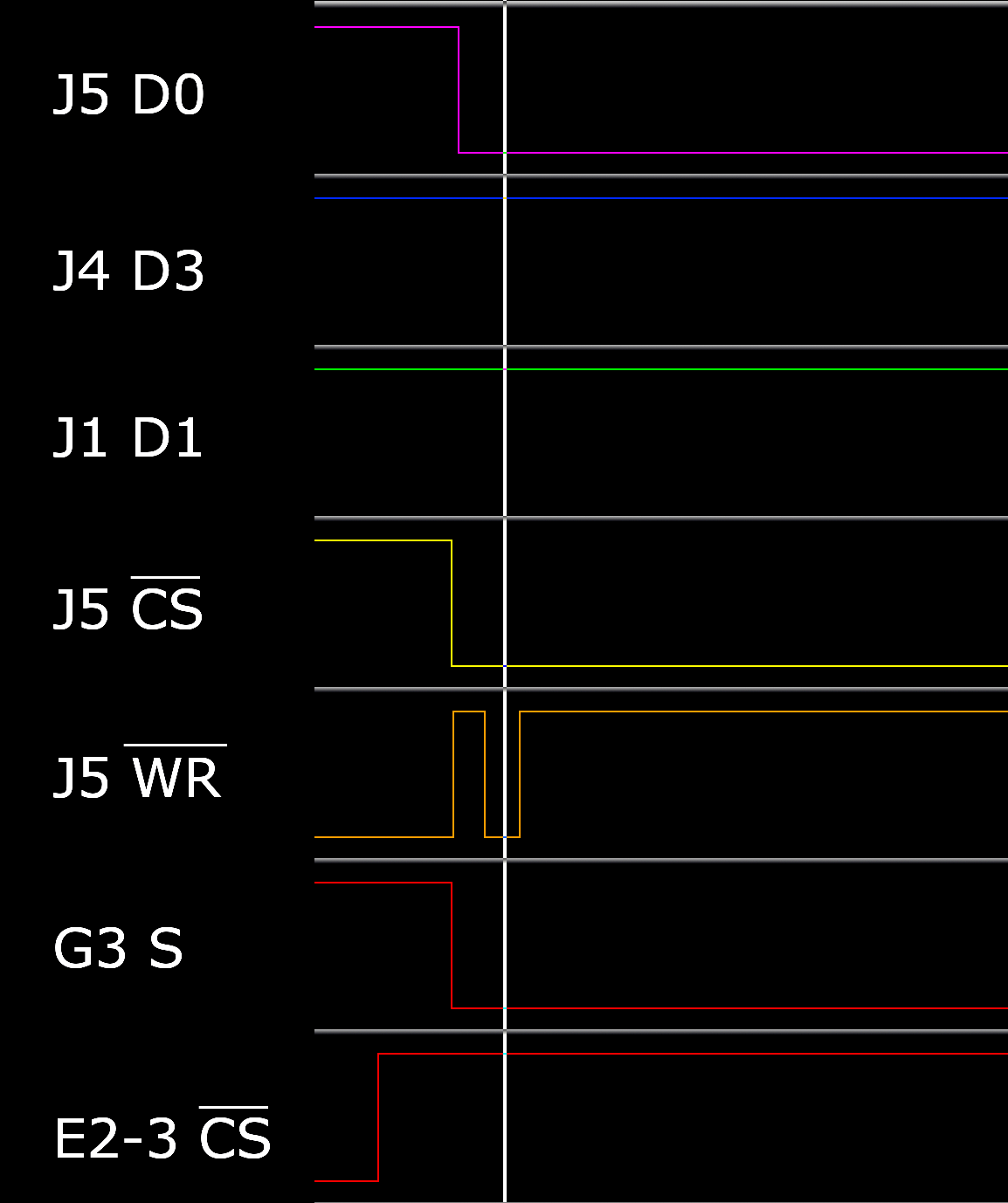
That was it! The low signal on one of the J5 data lines combined with the low J5 chip select and write signals indicates that this is a timestamp where the sprite is being rendered and the J1 and J4 bits should have also been low. However, E2-3 was disabled by its high chip select signal, so it did not output data.
The CS signal for E2-3 is fed from a signal called ENPOR that is output from a 74ls157 at D2.
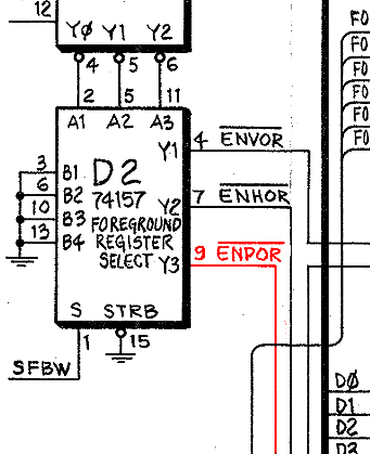
I probed this chip and immediately saw this was the culprit.
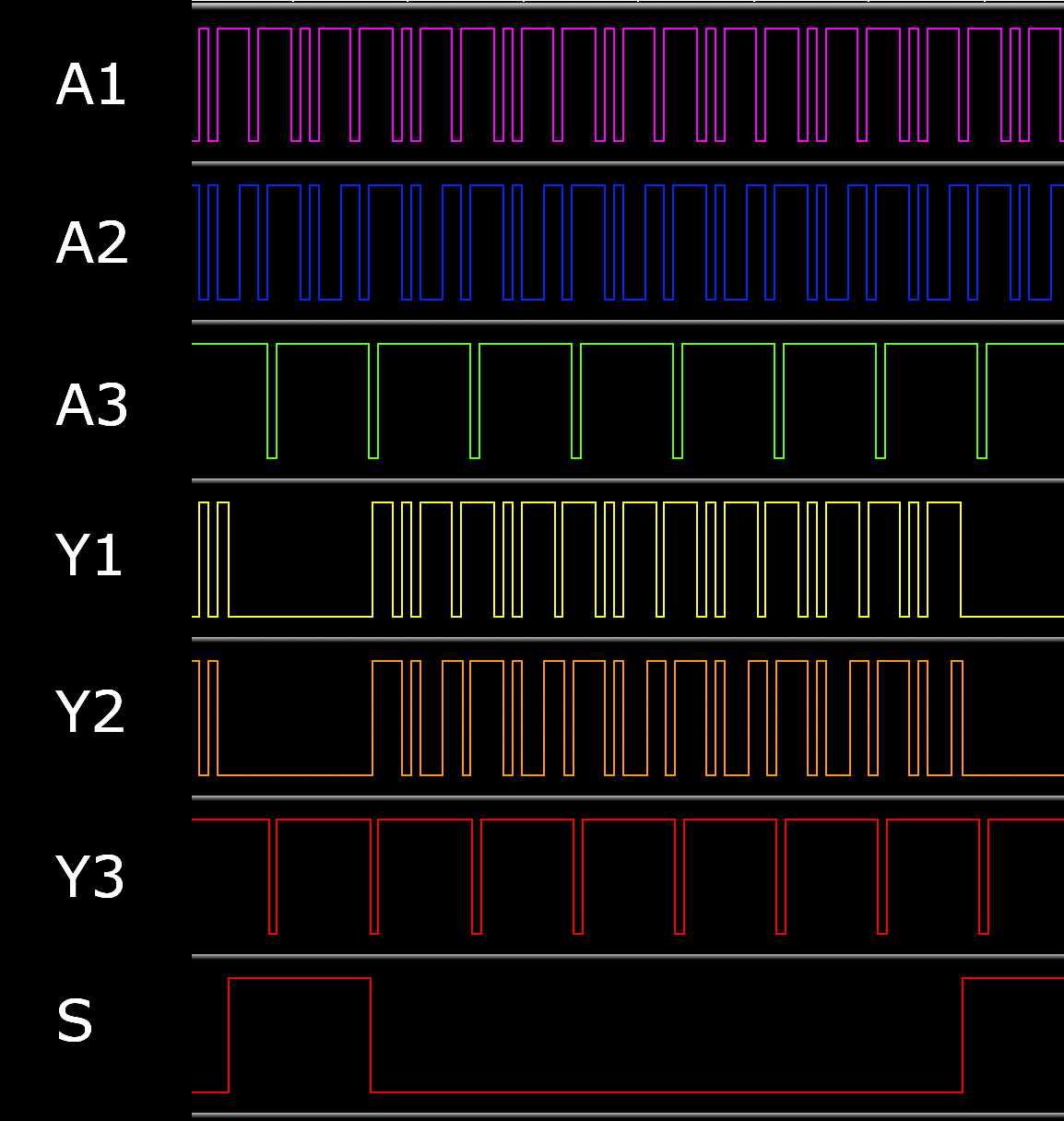
Whenever 'S' is high, a 74ls157 should send 'B' signals to the 'Y' outputs, which, for D2, are all tied low to ground. Y3 should have gone low for the duration of the two positive S pulses shown, similar to Y1 and Y2, but instead, it continued to output the value from A3.
I replaced D2 with a new 74ls157 and foreground video was also now fixed!